Overview
I wanted to understand how a computer actually executes instructions at the lowest level—not using a microcontroller, but by building the core components myself.
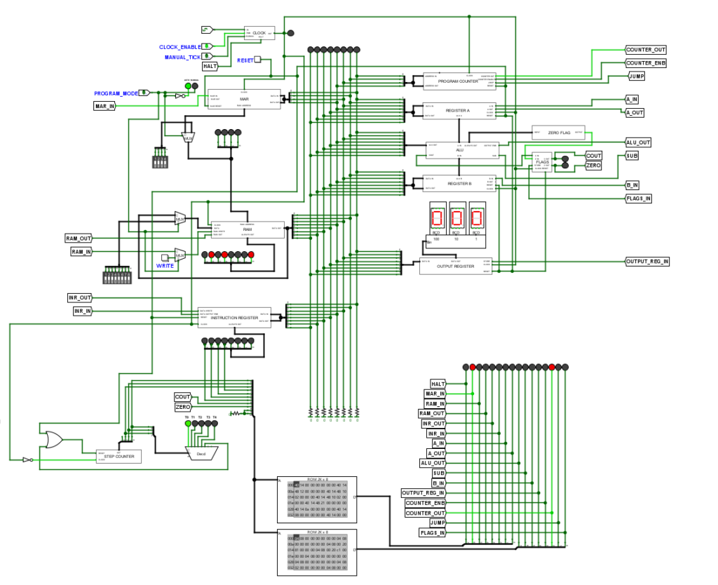
This project is an 8-bit computer designed and simulated in Logic Evolution, inspired by classic breadboard computers. Instead of just following a build, I focused on understanding how data flows through the system and how control signals coordinate execution.
The result is a working microcoded CPU that can fetch, decode, and execute instructions step by step.
What This System Does
This is a complete 8-bit CPU that:
- Fetches instructions from memory
- Decodes them using control logic
- Executes operations through an ALU
- Stores and transfers data between registers
The system follows a basic fetch–decode–execute cycle, similar to real processors.
Architecture
The design follows a simple Von Neumann-style architecture where program instructions and data share the same memory.
The system is divided into two main parts:
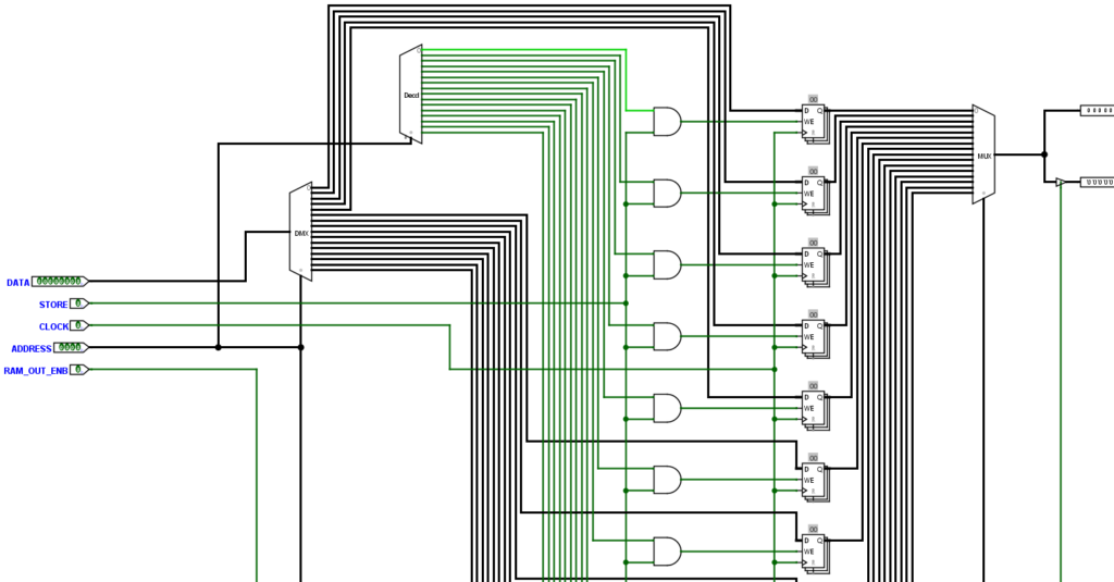
Datapath
Handles movement and processing of data:
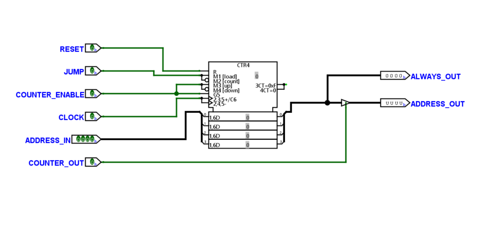
- Program Counter (PC)
- Memory Address Register (MAR)
- RAM
- Instruction Register (IR)
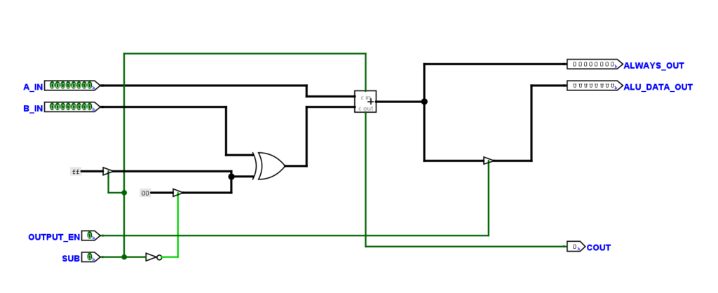
- Register A and Register B
- Arithmetic Logic Unit (ALU)
- Output Register
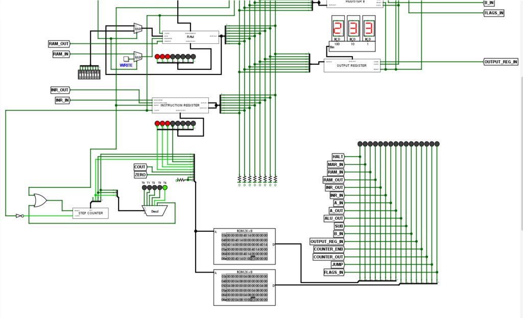
Control Unit
Controls how the datapath operates:
- Microcode ROM
- Step Counter (T-states)
- Decoder logic
- Control signals (read, write, load, enable, etc.)
All operations in the system are coordinated through control signals generated by the microcode.
Instruction Execution
Each instruction is executed in multiple steps using timing states (T1, T2, T3…).
A typical instruction cycle:
- Fetch
- PC → MAR
- Memory → Instruction Register
- Decode
- Instruction is interpreted
- Control signals are selected
- Execute
- Data is moved between registers
- ALU performs operation
- Results are stored
This step-by-step execution is controlled entirely through microcode.
Microcode and Control Logic
Instead of hardwiring control signals, this system uses microcode stored in ROM.
Each instruction maps to a sequence of control signals across multiple clock cycles.
This approach allows:
- Flexible instruction design
- Clear separation between datapath and control
- Easier debugging and modification
Control signals include:
- Register load/enable
- Memory read/write
- ALU operation selection
- Program counter control (increment/jump)
Instruction Set
The CPU supports a basic 4-bit opcode instruction set, designed to perform arithmetic, memory operations, and control flow.
Each instruction consists of:
- 4-bit opcode
- 4-bit operand (address or immediate value)
Opcode Table
Opcode  Mnemonic  Description
------  --------  -------------------------------------------
0000    NOP       No operation
0001    LDA       Load A register with contents of memory
0010    ADD       Add contents of memory to A register
0011    SUB       Subtract contents of memory from A register
0100    STA       Store contents of A register into memory
0101    LDI       Load immediate value into A register
0110    JMP       Jump to specified address
0111    JC        Jump if Carry flag is set
1000    JZ        Jump if Zero flag is set
1110    OUT       Load output register with A register
1111    HLT       Halt execution
Unused opcodes are reserved for future instruction expansion.
Example Program: Fibonacci Sequence
To validate instruction execution, a Fibonacci sequence program was implemented.
Program (Hex Representation)
51 4E 50 4F E0 1E 2F 4E E0 1F 2E 7D 63 60 00 01
What This Program Does
- Initializes starting values
- Repeatedly adds previous numbers
- Stores intermediate results in memory
- Outputs values using the OUT instruction
- Uses conditional jumps (JC/JZ) for control flow
This demonstrates:
- Arithmetic operations using ALU
- Memory read/write using LDA/STA
- Control flow using JMP, JC, JZ
- Output handling through OUT register
The correct execution of this program confirms that:
- Instruction decoding is working
- Microcode sequencing is correct
- Datapath and control unit are properly synchronized
Demonstration
The system successfully executes simple programs by:
- Loading instructions into memory
- Running step-by-step execution using clock pulses
- Displaying output through registers
The internal state of the CPU (register values, control signals) can be observed in real time within the simulator.
Gallery
Here are snapshots from the CPU design and simulation.
- Complete datapath and control wiring
- Microcode ROM and control signal mapping
- Instruction execution in progress
These visuals show how different components interact during instruction execution.
Challenges Faced
- Managing complex wiring between datapath components
- Designing correct control signal sequences for each instruction
- Debugging incorrect instruction execution due to timing issues
- Synchronizing step counter with microcode output
- Ensuring correct data flow between registers and ALU
Understanding and fixing these issues required careful tracing of signals across multiple clock cycles.
What I Learned
- How a CPU is built from basic digital components
- Difference between datapath and control unit
- How microcode simplifies control logic design
- Instruction execution at hardware level
- Importance of timing and synchronization in digital systems
Tools Used
- Logic Evolution (digital logic simulator)
- Digital logic components (registers, ALU, ROM, counters)
This project helped me understand how computers actually work internally, from instruction execution to control signal generation, and gave me hands-on experience with CPU design at the logic level.